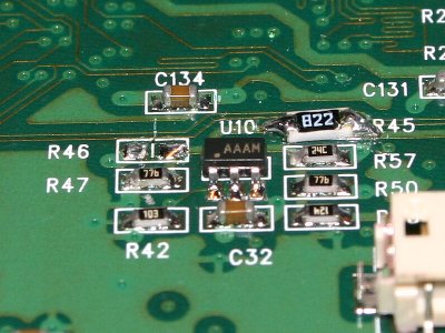
Modified Sitsang board showing R46 removed and R45 replaced with a 8.2K resistor. Note that a 0603 size SMT resistor was not available for R45; however there is ample space for a much larger resistor.
Dynamic voltage scaling is a useful technique for power consumption by reducing the processor's core voltage at runtime. Although the Intel Sitsang development board provides some support for DVS, some modifications are necessary to make full use of its capabilities. The instructions below describe how to enable DVS support on a Sitsang board.
The Sitsang board comes with two MAX5360 Digital-to-Analog Converters. These DACs are addressable over the XScale's on-board I2C bus, and have a voltage range of 0-2.0V. To limit the output voltage range, each DAC output contains three resistors, which scale the output voltage to 0.83V-0.91V.
| DAC | I2C Address | Part # | IC | Limiting Resistors | |
| A | 0x60 | MAX5360LEUK | U13 | R45-47 | |
| B | 0x62 | MAX5360MEUK | U14 | R50,56,57 | (Selected at Boot) |
A MAX4544 Analog Switch (U10) selects between the output voltages of the two DACs. The analog switch is controlled by the on-board Xilinx CPLD (U24).
The VCC_CORE suppy for the XScale is regulated by a MAX1820 (U12). The MAX1820 takes the reference voltage selected by the analog switch, and has a gain of 1.76, resulting in a voltage range of 1.46V to 1.60V, which is too high to be usable for dynamic voltage scaling.
In order to to useful DVS research on the Sitsang, we must first make modifications to both the hardware and software:
The Sitsang board comes with resistors which limit the range of voltage scaling to a safe range of 1.46V to 1.60V. However, in order to perform useful DVS, we must be able to scale the core voltage down to the XScale's minimum of 1.0V (and possibly lower). To do so, we must modify two resistors on the Sitsang board. We will only modify the resistors on DAC A, the one NOT selected at startup, thus the Sitsang will still boot with the normal core voltage of 1.46V.
| Resistor | Old Value | New Value |
| R45 | 120K | 8.2K |
| R46 | 17.4K | None |
This modification will change the core voltage range to 0.0V to 1.5V when DAC A is selected. Higher voltages may be obtained by choosing a resistance lower than 8.2K, however the XScale processor is rated for a maximum voltage of 1.6V.
R45 and R46 are located behind the battery on the bottom side of the Sitsang. To access them, unscrew the rear panel, and unplug the battery from connector J14.
Modified Sitsang board showing R46 removed and R45 replaced with a 8.2K
resistor. Note that a 0603 size SMT resistor was not available for R45;
however there is ample space for a much larger resistor.
The MAX4544 Analog Switch is controlled by the Xilinx CPLD (U24). However, the
CPLD is programmed to only allow a voltage change when the CPU is in sleep
mode. In order to have full control of the analog switch, we will change
the behavior of the VCC_CHANGE bit (bit 11) in the
PCR register (0x08000000) so that writing a 0 or 1 to it will
directly select the DAC.
Note: In the kernel code and Sitsang documentation, bit 11 of the
PCR register is referred to as the VCC_CHANGE bit.
However, in the VHDL code, bit 11 is named REG_PCR_DELAY_WAKEUP.
Intel's VHDL code was developed using the Xilinx Webpack 4.2WP2.x. Version 4.2WP3.x may be downloaded for free from Xilinx's web site, and I have successfully used it for generating the Sitsang CPLD logic.
To make the changes, first copy the CPLD code from the Intel CD-ROM. It can
be found in the Hardware and Related Documentation/Hardware
Design/CPLD/SitsangCPLD.npl, in Xilinx Webpack, and edit the SitsangCPLD.vhd
file. To make the VCC_CHANGE bit directly select between the
two DACS, remove the code inside the Power_Logic block, and
replace it with the following:
Power_Logic : Block
Begin
  Vcc_Core_Ref_SW <= '1' when (Globe_nReset_In = '1') and
    (REG_PCR_DELAY_WAKEUP = '1') else '0';
  Xs_Wakeup <= '0';
End Block Power_Logic;
The Xilinx software may then be used to generate a JEDEC (.jed) file which is used to program the CPLD. However, since space in the CPLD is extremely tight, the fitter may fail due to the changes. To get around this, we can remove some of the unnecessary code, such as that for the LED registers.
The CPLD may be reprogrammed using the Sitsang's JTAG cable and the software
programming utility provided with Xilinx Webpack. The
sitsang_PXA255.cdf file provides the proper configuration for
programming the CPLD on the Sitsang board. I have had success doing
this under Windows XP. The software once failed with strange errors, but
it was easily fixed by rebooting the system.
The sitsang-dvs kernel module provides direct access to the
voltage scaling hardware on the Sitsang board. It may be downloaded in
source code format, sitsang-dvs.c, or as a
binary module, sitsang-dvs.o, compiled against
the 2.4.19-rmk4-pxa2-alvin2 kernel provided on the Intel CD-ROM.
To use the sitsang-dvs module, upload it to the Sitsang board
as use insmod sitsang-dvs to load it. NOTE: Do not use the
XScale I2C modules while using the sitsang-dvs module. The
sitsang-dvs module provides a minimal I2C implementation for
communicating with the on-board DACs.
Once loaded, the module creates a file in the /proc directory
named vcc_core. This module provides access to the two DACs and
the analog switch. The module accepts three commands:
S - Switch to DAC A
A<value> - Set the value of DAC A, where
<value> is from 0-255
B<value> - Set the value of DAC B, where
<value> is from 0-255
The A and B commands take a value from 0 to 255.
However, since the MAX5360 DACs are only support 6 bits, the two lowest bits
of the value should always be 0. With the PCB modifications on DAC A using
an 8.2K resistor, the following table lists some possible voltage/value
combinations:
| Voltage | DAC A Value | DAC B Value | Max. CPU Frequency |
| 0.70 V | 120 | - | - |
| 0.80 V | 136 | - | - |
| 0.90 V | 152 | - | - |
| 1.00 V | 168 | - | 199 MHz |
| 1.10 V | 188 | - | 299 MHz |
| 1.20 V | 204 | - | 299 MHz |
| 1.30 V | 220 | - | 398 MHz |
| 1.40 V | 236 | - | 398 MHz |
| 1.46 V | 248 | 0 | 398 MHz |
| 1.50 V | 252 | 80 | 398 MHz |
| 1.60 V | - | 252 | 398 MHz |
The maximum CPU frequencies listed above are taken from the Intel datasheets. Frequencies higher than those listed may still result in stable operation.
So, the Sitsang boots at the default CPU frequency of 398 MHz. To enable DVS and set the processor to lowest allowed core voltage of 1.30 V:
$ echo A220 > /proc/vcc_core
Wrote value 0xdc (220) to I2C address 0x60 (96).
$ echo S > /proc/vcc_core
VCC_CORE DAC A selected.
Note that a value must be written to DAC A before the S command
is issued. Otherwise, the core voltage will be switched to 0 V, and the
processor will immediately halt.
Next, to switch the processor to 99 MHz at the lowest core voltage of 1.0 V:
$ echo 99000 > /proc/sys/cpu/0/speed
Changing CPU frequency to 99 Mhz (PXbus=50Mhz).
$ echo A168 > /proc/vcc_core
Wrote value 0xa8 (168) to I2C address 0x60 (96).
Last Modified: 8/3/04 by lcs@cc
Return to Intel Sitsang Resources |
Leo Singleton